Address many molecular features in parallel.
Increase molecular density while preserving the designed identity and location of every probe.

The DNA chip platform
Centrillion brings semiconductor-scale manufacturing to molecular measurement. Through photolithographic synthesis, Centrillion’s light-directed synthetic biology platform writes many different DNA probe sequences at known positions on a wafer, creating a programmable foundation for biological assays.
Light-directed synthetic biology
A photomask selects which features receive UV exposure. Light removes the protecting group. The next DNA base couples only where the light landed. Repeat.
Because selection is optical, millions of features can be addressed in parallel during each synthesis cycle.
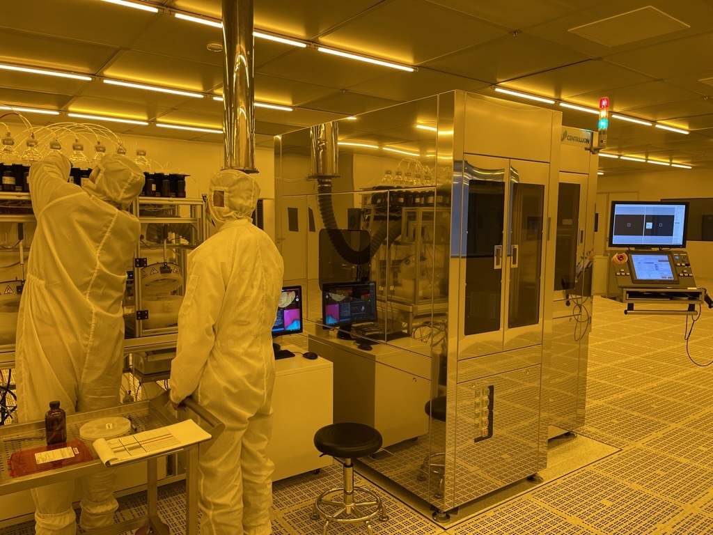
Wafer-scale production
The Centrillion lithography facility brings optical patterning, surface chemistry, and wafer processing into one production environment. Yellow safe-light conditions protect photosensitive process steps while the tools create densely patterned DNA surfaces.
Technology for synthesis
Why it scales
Printed arrays add features through additional deposition events. In a photolithographic array, one exposure patterns many selected features at once. The synthesis cycle is governed primarily by probe length rather than by the number of different probes on the surface.
That parallel process connects molecular density to the control methods of wafer manufacturing: alignment, surface chemistry, metrology, and repeatable processing across many chips.
Today, more than 2.4 billion distinct DNA features can be synthesized on a single wafer. Each feature contains sufficient DNA molecules to support robust detection, dynamic range, and analytical accuracy.
Programmable at the molecular level
Every feature is defined by both its sequence and its coordinate. Changing the design changes which molecular questions the chip can ask while preserving a shared manufacturing process.
Probe content, chip geometry, surface chemistry, assay workflow, and readout remain configuration specific. The common foundation is a densely patterned, addressable molecular surface.
Arrays with Gray-code zip codes can also incorporate flexible, user-designed capture sequences, allowing the same spatial framework to be adapted for multiomics and other applications.
Increase molecular density while preserving the designed identity and location of every probe.
Change probe content, chip format, and analytical workflow without giving up the manufacturing advantages of a shared wafer process.
Connect design, surface chemistry, process control, and wafer handling in a shared production system.
Start a conversation